Scanning Probe Microscopy/Atomic Force Microscopy (SPM/AFM Analysis) Laboratory
Scanning probe microscopy (SPM) refers to a family of measurement techniques that utilize a scanning probe. The most common measurement is Atomic Force Microscopy (AFM Analysis), which measures surface topography. Imaged areas can be from the nm scale to as large as 100 µm X 100 µm. Heights and depths of features can be measured
and many surface roughness parameters, e.g Ra, can be calculated. 3-D images can also be produced for dramatic data presentation. Magnetic and electrical response can also be measured with SPM.

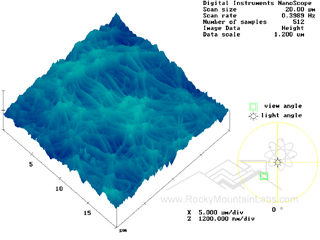
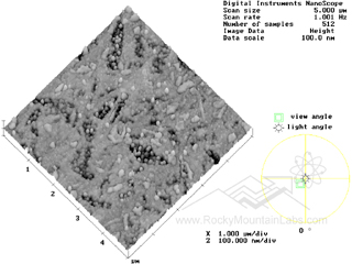
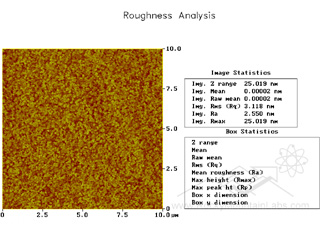
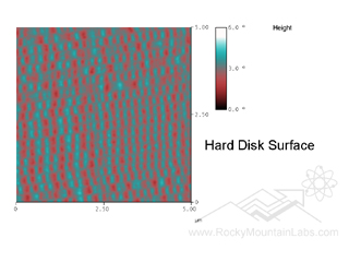
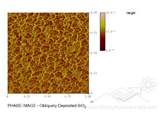
Scanning Probe Microscopy (SPM), Atomic Force Microscopy (AFM Analysis)
Description
Scanning Probe Microscopy (SPM) Analysis refers to a group of techniques used to measure mechanical, magnetic, electrical, and electrochemical surface topography on a nanometer scale. It can measure features from as small as interatomic spaces to a tenth of a millimeter. The three dimensional resolution of SPM is unparalleled by any other technique.
The ability to measure surfaces in three dimensions provides information that cannot be obtained with optical or typical electron microscopes. Unlike many stylus profilometers that only scan in a straight line, SPMs raster over a square area and give better and more precise topographical data.
SPMs can be operated in air and liquids. This allows for the examination of a very extensive range of materials and environments, generally with no sample preparation. Examinations of biological materials can be carried out in appropriate solutions to preserve their vital characteristics.
Applications
SPM is applied to problems in many industries from space materials testing to semiconductor fabrication to compact disk manufacturing. A few examples include:
- silicon wafer roughness
- compact disk texture
- polymer membrane imaging
- biological structure imaging
- cancer research
- biomedical pathology
- immunoassay process development
- thin film and coating
- integrated optics
- particle/surface forces
- nucleation
- contact lenses
- catalysis
Types of data/output:
- high resolution color images
- surface roughness
- grain size
- cross sections
- fractal roughness
- bearing ratios
- microsurface area
- particle counting
Data can be supplied as hard copy or in digital files for electronic transfer and further processing by the client.
Sample Requirements
SPM can analyze solids, including biomaterials. Generally , no costly sample preparation or coating is required, since both conductive and nonconductive samples can be imaged. Usually, smooth samples are best and those that have macroscopic roughness with greater that 5 µm maximum relief cannot be analyzed. Sample sizes up to 8 inches in diameter may be analyzed.
To obtain the most accurate results, surface features should not be mobile, because the stylus could potentially move them giving erroneous position information.
Analysis times are in the order of thirty to sixty minutes dependent upon sample characteristics. Since SPM is a nondestructive technique, Rocky Mountain Laboratories can combine it with other analytical methods for subsequent analysis on the same sample to provide complementary information.
Stylus Profilometry
In this technique, roughness and the sizes of surface features are measured by the mechanical movement of a diamond stylus over the sample. The trace of the surface is digitized and stored in a computer for display on a CRT and output to a printer. The stylus force can be adjusted to protect fragile surfaces from damage. The Stylus Profilometer can measure laterally to 1 µm and vertically to 5 Å with effective magnification of 20-100,000X. It provides good two dimensional topographical data and is nondestructive.
Note:
*NanoScope™ and TappingMode™ are registered trademarks of Bruker, Inc.
What is Scanning Probe Microscopy/Atomic Force Microscopy (SPM/AFM Analysis)?
Scanning Probe Microscopy (SPM) Analysis and Atomic Force Microscopy (AFM) Analysis are imaging techniques used in materials science to obtain high-resolution images of surfaces at the atomic and molecular scales.
In SPM, a tiny probe with a sharp tip is scanned across the surface of a sample, and the interactions between the probe and the surface are measured. This can be done in a number of ways, including measuring the current flowing between the probe and the sample (Scanning Tunneling Microscopy or STM) or measuring the force between the probe and the sample (Atomic Force Microscopy or AFM).
AFM is a type of SPM that uses a small cantilever with a sharp tip to scan across the surface of a sample. As the tip moves across the surface, it is deflected by the forces between the tip and the surface. These deflections are measured using a laser or other optical system, and are used to generate an image of the surface topography.
AFM Analysis Laboratory can be used to image a wide range of materials, from metals and semiconductors to polymers. It can also be used to measure a variety of physical properties, including surface roughness, adhesion, and elasticity.
SPM/AFM analysis is a powerful tool in materials science and nanotechnology research, providing researchers with detailed images and measurements of surfaces at the atomic and molecular scale.
How does Scanning Probe Microscopy/Atomic Force Microscopy (SPM/AFM Analysis) work?
Scanning Probe Microscopy (SPM) and Atomic Force Microscopy (AFM) work by using a small probe with a sharp tip to scan across the surface of a sample. The probe is positioned extremely close to the surface of the sample, and the interactions between the probe and the surface are measured.
In AFM, the probe is typically mounted on a small cantilever, which is suspended over the sample. As the cantilever is scanned across the surface of the sample, it is deflected by the forces between the probe and the surface. These deflections are measured using a laser or other optical system, and are used to generate an image of the surface topography.
The probe tip is positioned so that it is very close to the surface of the sample, but not touching it. When the tip is moved across the surface, it interacts with the atoms and molecules on the surface, and these interactions cause the cantilever to deflect. The amount of deflection is measured by bouncing a laser beam off the back of the cantilever, and the deflection is recorded as a signal.
The signal is then used to create an image of the surface topography. The height of the surface features is determined by the amount of deflection of the cantilever. The image is generated by scanning the probe tip across the surface in a series of parallel lines, similar to the way that a television image is generated.
In addition to generating images, AFM can also be used to measure a variety of physical properties, including surface roughness, adhesion, and elasticity. By applying a force to the probe tip and measuring the resulting deflection, researchers can determine the mechanical properties of the sample, such as its stiffness or hardness.
Scanning Probe Microscopy/Atomic Force Microscopy (SPM/AFM Analysis) Process
The process for Scanning Probe Microscopy (SPM) and Atomic Force Microscopy (AFM) analysis typically involves the following steps:
- Sample preparation: The sample must be prepared in such a way that it is clean and flat. Depending on the nature of the sample, this may involve cleaning with solvents, polishing with abrasives, or coating with a thin layer of metal.
- Mounting the sample: The sample is mounted onto a holder or stage that can be positioned precisely in three dimensions. This allows the probe tip to be brought into close proximity to the sample.
- Probe selection: The type of probe used will depend on the specific application. Probes can be made from a variety of materials, including silicon, diamond, or tungsten.
- Calibration: Before the measurement process begins, the probe must be calibrated to ensure that it is working correctly. This involves measuring the probe tip shape and determining its spring constant.
- Scanning the sample: The probe is positioned close to the surface of the sample and is then scanned across the surface in a series of parallel lines. As the probe tip moves across the surface, the deflection of the cantilever is measured, and an image of the surface topography is generated.
- Analyzing the data: The data generated by the SPM/AFM is typically analyzed using specialized software that can process the raw data and generate a detailed image of the surface topography. This may involve filtering the data to remove noise or other artifacts.
- Interpreting the results: The final step in the SPM/AFM process is to interpret the results and draw conclusions about the properties of the sample. This may involve comparing the SPM/AFM data with other measurements, such as electron microscopy or spectroscopy data, to gain a more complete understanding of the sample.
Principles of Scanning Probe Microscopy/Atomic Force Microscopy (SPM/AFM Analysis)
The principles of Scanning Probe Microscopy (SPM) and Atomic Force Microscopy (AFM) are based on the interaction between a sharp probe tip and the surface of a sample. The tip is mounted on a cantilever and is positioned close to the surface of the sample. As the tip is scanned across the surface, the interaction between the tip and the sample causes the cantilever to deflect.
There are different types of SPM, such as Scanning Tunneling Microscopy (STM), which measures the current that flows between the tip and the sample, and Atomic Force Microscopy (AFM), which measures the force between the tip and the sample. However, the basic principles are similar.
The deflection of the cantilever is measured using a laser or other optical system, and is used to generate an image of the surface topography. The tip can also be used to apply a force to the sample, allowing researchers to measure a variety of physical properties such as surface roughness, adhesion, and elasticity.
The resolution of SPM/AFM is limited by the sharpness of the probe tip and the stability of the cantilever. To achieve high resolution, the cantilever must be very stable and must be able to detect very small deflections. The probe tip must also be sharp and must be positioned very close to the surface of the sample.
SPM/AFM is a powerful technique for imaging and characterizing surfaces at the atomic and molecular scale. It has applications in a wide range of fields, including materials science, physics and chemistry and is used to study a variety of materials, including metals, semiconductors and polymers.
Applications of Scanning Probe Microscopy/Atomic Force Microscopy (SPM/AFM Analysis)
Scanning Probe Microscopy (SPM) and Atomic Force Microscopy (AFM) are versatile techniques that can be used to investigate a wide range of materials and surface properties. Some of the applications of SPM/AFM include:
- Surface topography imaging: SPM/AFM can generate high-resolution images of surface topography, allowing researchers to visualize surface features at the atomic and molecular scale. This is useful for studying the morphology of materials, such as the structure of crystals, the arrangement of molecules in a polymer, or the topology of a biological membrane.
- Surface roughness analysis: SPM/AFM can be used to measure the roughness of a surface, which is important for many applications, such as in the semiconductor industry, where smooth surfaces are necessary for device fabrication.
- Surface charge measurement: SPM/AFM can measure the electrostatic force between the probe and the surface of the sample, allowing researchers to investigate the charge distribution on the surface.
- Adhesion force measurement: SPM/AFM can measure the adhesion force between the probe and the sample, which is useful for investigating the adhesive properties of materials, such as in the development of adhesives or coatings.
- Materials characterization: SPM/AFM can be used to investigate a variety of materials, including metals, semiconductors, polymers, and ceramics. This is important for understanding the properties of these materials and developing new materials with specific properties.
SPM/AFM is a powerful tool for investigating the properties of surfaces and materials at the nanoscale, and has a wide range of applications in materials science, physics and chemistry.
Where is Scanning Probe Microscopy/Atomic Force Microscopy (SPM/AFM Analysis) used?
Scanning Probe Microscopy (SPM) and Atomic Force Microscopy (AFM) are used in a variety of fields where high-resolution imaging and characterization of surfaces are required. Some of the areas where SPM/AFM is commonly used include:
- Materials science: SPM/AFM is used extensively in materials science to investigate the properties of surfaces and materials at the atomic and molecular scale. This is important for developing new materials with specific properties, such as in the semiconductor industry, where SPM/AFM is used to study the surface of silicon wafers.
- Nanotechnology: SPM/AFM is a key tool in nanotechnology, allowing researchers to manipulate and characterize nanoscale materials and devices. This is important for developing new technologies, such as in the field of nanoelectronics.
- Surface chemistry: SPM/AFM is used to investigate the surface chemistry of materials, such as the adsorption of molecules on surfaces. This is important for understanding chemical reactions on surfaces, such as in catalysis and corrosion.
- Tribology: SPM/AFM is used in tribology to study the friction and wear of materials, such as in the development of lubricants and coatings.
SPM/AFM is a versatile tool that is used in a wide range of applications where high-resolution imaging and characterization of surfaces are required. Its ability to investigate surfaces at the atomic and molecular scale makes it an important tool in materials science, nanotechnology and many other fields.
Industries which need Scanning Probe Microscopy/Atomic Force Microscopy (SPM/AFM Analysis)
Scanning Probe Microscopy (SPM) and Atomic Force Microscopy (AFM) are used in many industries where high-resolution imaging and characterization of surfaces are important. Some of the industries that commonly use SPM/AFM include:
- Semiconductor industry: The semiconductor industry uses SPM/AFM extensively to investigate the surface of silicon wafers and other materials used in semiconductor device fabrication. This is important for understanding the properties of the materials and optimizing the manufacturing process.
- Materials science industry: The materials science industry uses SPM/AFM to investigate the properties of a wide range of materials, including metals, ceramics, polymers, and composites. This is important for developing new materials with specific properties and improving the performance of existing materials.
- Nanotechnology industry: The nanotechnology industry uses SPM/AFM to manipulate and characterize nanoscale materials and devices. This is important for developing new technologies, such as in the field of nanoelectronics.
- Coatings industry: The coatings industry uses SPM/AFM to investigate the properties of coatings, such as adhesion, wear resistance, and surface roughness. This is important for developing new coatings with specific properties and optimizing the performance of existing coatings.
- Aerospace industry: The aerospace industry uses SPM/AFM to investigate the properties of materials used in aircraft and spacecraft, such as metals and composites. This is important for ensuring the safety and reliability of these materials in extreme environments.
SPM/AFM is a valuable tool for many industries where high-resolution imaging and characterization of surfaces are required. Its ability to investigate surfaces at the atomic and molecular scale makes it an important tool in materials science, nanotechnology, biotechnology, and many other fields.
Strengths and Limitations of Scanning Probe Microscopy/Atomic Force Microscopy (SPM/AFM Analysis)
Scanning Probe Microscopy (SPM) and Atomic Force Microscopy (AFM) have many strengths and limitations. Some of the key strengths and limitations are:
Strengths:
- High resolution: SPM/AFM can achieve extremely high resolution imaging, with the ability to resolve individual atoms and molecules on a surface.
- Non-destructive: SPM/AFM is a non-destructive imaging technique, allowing samples to be imaged without damaging them.
- Versatility: SPM/AFM can be used to investigate a wide range of materials, including metals, semiconductors, polymers, and biological samples.
- Quantitative measurements: SPM/AFM can be used to make quantitative measurements of surface properties, such as roughness and friction.
- In situ imaging: SPM/AFM can be used for in situ imaging, allowing researchers to investigate surface properties under different environmental conditions.
Limitations:
- Limited scan size: SPM/AFM is a scanning technique, and the size of the scan area is limited. This makes imaging large samples time-consuming.
- Surface damage: Although SPM/AFM is non-destructive, it can still cause surface damage if the tip is not properly controlled.
- Tip wear: The tips used in SPM/AFM can wear down quickly, which can affect the quality of the images obtained.
- Sample preparation: SPM/AFM requires careful sample preparation, including cleaning and mounting the sample, which can be time-consuming and difficult.
- Limited chemical information: SPM/AFM provides information on surface topography and properties, but it does not provide chemical information about the sample.
SPM/AFM is a powerful tool for investigating surface properties at the atomic and molecular scale, but it has some limitations that need to be considered when using this technique.

