Surface cleanliness is critical throughout semiconductor wafer processing. Even small amounts of contamination can interfere with lithography, deposition, etching, oxidation, bonding, and other fabrication steps. Organic films, metallic particles, chemical residues, and airborne particulates can affect surface properties, create defects, and reduce process consistency.
Oxide and other inorganic films: Unintended surface oxidation, deposited inorganic material, or process byproducts can alter the surface chemistry. These changes may affect contact resistance, bonding, or the behavior of subsequent processing steps.
How Surface Contamination Affects Wafer Processing
Contamination can create problems at multiple stages of semiconductor manufacturing. During photolithography, organic films and particles may interfere with resist coating, exposure, and pattern transfer. This can contribute to poor adhesion, coating defects, or localized pattern irregularities.
During deposition and surface treatment, contamination may prevent uniform film formation or affect the interface between the deposited layer and the underlying wafer. Residual material can also influence etching behavior, resulting in inconsistent material removal.
Metallic contamination is particularly important because certain metals can introduce electrically active defects or affect semiconductor device performance. Even when contamination is localized, it may create reliability concerns depending on its composition, concentration, and position within the device structure.
Contamination can also affect wafer bonding and packaging processes. Organic residues, particles, and unintended oxide layers may interfere with intimate surface contact, contributing to weak bonding or interface defects.
Common Sources of Wafer Surface Cleanliness Problems
Identifying the source of contamination is often more challenging than detecting the presence of a deposit.
Cleaning processes are one possible source. Incorrect chemical concentrations, exhausted cleaning solutions, inadequate rinsing, or incomplete drying can leave unwanted material on the wafer. Residues may also form when cleaning chemicals react with contaminants already present on the surface.
Processing equipment can introduce contamination through contact with chamber components, wafer handling mechanisms, seals, fixtures, and other materials. Wear or degradation of equipment components may release particles or chemical residues during repeated processing cycles.
Handling and storage are additional considerations. Contamination can be introduced through wafer carriers, packaging materials, gloves, handling tools, or exposure to airborne particles. Cross-contamination between process steps may also occur when residues are transferred from one wafer or piece of equipment to another.
A useful investigation compares affected wafers with clean reference wafers, examines whether contamination is localized or widespread, and considers the process steps immediately preceding the appearance of the defect.
Why Surface Chemistry Analysis Is Important
Routine visual inspection and particle monitoring can identify some cleanliness problems, but they do not necessarily reveal the chemical identity of a thin surface film or trace contamination.
Analytical testing can help determine whether a wafer contains organic compounds, metallic elements, inorganic deposits, or changes in surface chemistry. This information helps process engineers distinguish between different contamination mechanisms and evaluate potential sources.
For example, an organic film may point toward residual photoresist, polymer degradation, or handling-related contamination. Metallic elements may suggest contact with equipment materials, process chemicals, or other sources. Surface oxidation may indicate exposure to reactive environments or changes during processing and storage.
The analytical method must be selected according to the type of contamination, the expected concentration, and the depth or area that needs to be examined.
What Analytical Techniques Can Be Used to Investigate Wafer Contamination?
Several analytical techniques can provide complementary information about wafer surface cleanliness.
X-ray Photoelectron Spectroscopy (XPS) is useful for identifying surface elements and evaluating their chemical states. It can help characterize thin oxide layers, organic contamination, and changes in surface chemistry. Because XPS is highly surface-sensitive, it is particularly valuable when contamination is confined to the outermost layers of a wafer.
Auger Electron Spectroscopy (AES) provides highly localized elemental analysis of wafer surfaces. It can help investigate small contaminated regions, surface segregation, and localized elemental deposits. AES is useful when engineers need to compare contaminated and unaffected areas.
Scanning Electron Microscopy (SEM) allows detailed examination of surface morphology and particulate contamination. It can reveal particle size, shape, distribution, and surface defects. When combined with Energy Dispersive X-ray Spectroscopy (EDS), SEM can also provide elemental information about particles and selected surface deposits.
Fourier Transform Infrared Spectroscopy (FTIR) can help identify organic residues, including polymeric films, oils, solvents, and other organic compounds. It is useful when the suspected contamination involves molecular materials rather than primarily metallic or inorganic deposits.
No single technique identifies every type of wafer contamination. Combining surface-sensitive chemical analysis with microscopy and molecular spectroscopy can provide a more complete understanding of the material present.
Distinguishing Surface Contamination from Process-Induced Surface Changes
Not every surface chemistry difference indicates contamination. Wafer processing intentionally changes surface composition during oxidation, deposition, etching, cleaning, and other operations.
The challenge is determining whether an observed surface layer is an expected result of processing or an unintended deposit.
Comparing affected wafers with process specifications, reference samples, and wafers from different production stages can help establish whether a change is abnormal. Analytical results should also be interpreted in the context of the wafer material, process history, cleaning conditions, and storage environment.
For very thin films, the underlying substrate may contribute to the analytical signal. Sample handling, exposure to air, and preparation procedures can also influence results. Careful sample preservation and appropriate analytical methods are therefore important.
How Rocky Mountain Labs Can Help
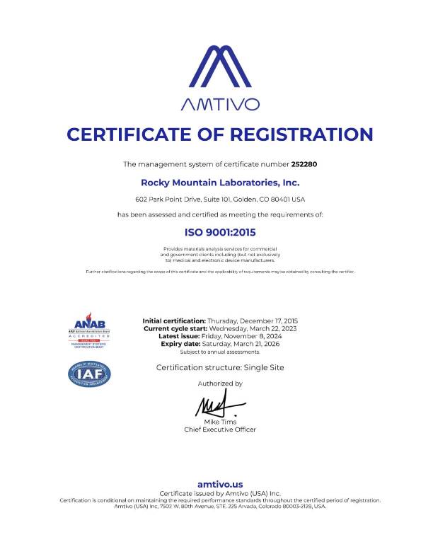
Rocky Mountain Labs provides analytical testing to help manufacturers investigate surface cleanliness issues and identify unknown materials on semiconductor wafers and related components.
Using techniques such as FTIR, SEM/EDS, AES, and XPS, the laboratory can help characterize organic residues, metallic particles, inorganic deposits, surface oxidation, and other forms of contamination. These methods provide information about the composition and characteristics of unwanted material, helping engineers investigate potential contamination sources.
Whether the issue involves unexplained wafer surface residues, metallic contamination, particulate deposits, or unexpected changes in surface chemistry, Rocky Mountain Labs can help determine what materials are present and provide analytical results to support further investigation and process improvement.